Assignments
PSY 315 Assignment Questions and Answers
ASSIGNMENT PSY315(SENSORY PROCESSES)
A. Draw, label and write out the functions of the following organs:
- The heart.
- The sense organ of sight.
- The sense organ of taste.
- The tactile organ.
- The sense organ of smell.
- The brain and its compartments.
- Animal cell.
- Plant cell.
- Neuron.
- The digestive system.
B. State the differences between plant and animal cell.
C. State fully the functioning of the neuron.
Requirement:Drawing book
Pencil
Eraser
Ruler
Sharpener
(We have just one month to do this assignment)
If you need detailed instruction on how to draw it then you can send a message with 500 Naira to get a detailed explanation of ho to draw it perfectly.
ANSWERS
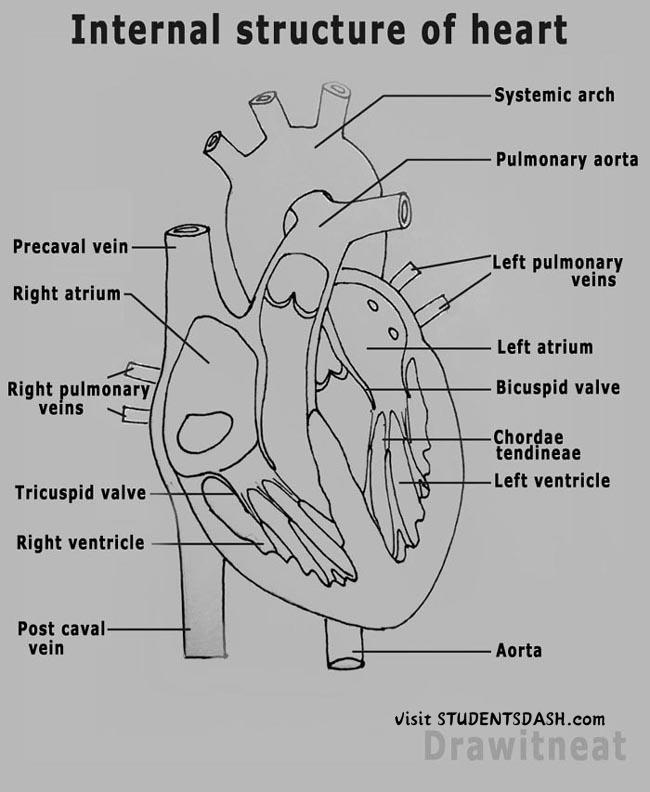
1. The Heart
Functions of the Heart:
- Pumps Blood – The heart circulates blood throughout the body, ensuring oxygen and nutrients reach all tissues.
- Supplies Oxygen & Nutrients – Oxygen-rich blood from the lungs is distributed to the body to support cell functions.
- Removes Waste Products – The heart helps transport carbon dioxide and other waste products to the lungs and kidneys for removal.
- Maintains Blood Pressure – By controlling the force and rate of blood flow, the heart regulates blood pressure.
- Supports Circulatory System – It works with blood vessels (arteries, veins, capillaries) to keep blood moving efficiently.
- Adapts to Body Needs – The heart beats faster during physical activity to supply more oxygen and slows down during rest.
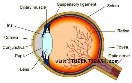
2. The Sense Organ of Sight (Eyes)
Functions of the Eyes:
- Detects Light – The eyes capture light and convert it into electrical signals for the brain to process.
- Enables Vision – Allows us to see objects, colors, shapes, and movements.
- Focuses on Objects – The lens adjusts to focus on near or distant objects.
- Helps in Depth Perception – Both eyes work together to determine distances between objects.
- Aids in Balance and Coordination – Vision helps maintain balance and guides movement.
- Protects Against Harm – Reflexes like blinking help shield the eyes from dust, bright light, and foreign objects.
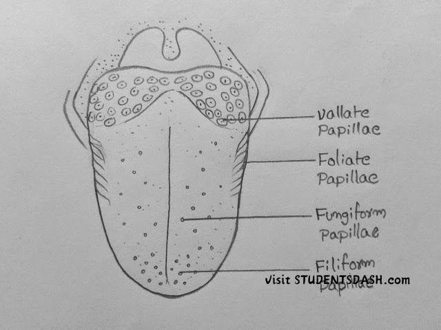
3. The Sense Organ of Taste (Tongue)
Functions of the Tongue:
- Detects Different Tastes – The tongue identifies sweet, sour, salty, bitter, and umami flavors using taste buds.
- Aids in Digestion – It helps move food around the mouth for chewing and mixing with saliva.
- Assists in Swallowing – The tongue pushes food towards the throat for swallowing.
- Enhances Flavor Perception – Works with the nose to fully experience flavors.
- Helps in Speech – The tongue plays a major role in forming words and sounds.
- Acts as a First Line of Defense – The tongue’s sensitivity helps detect spoiled or harmful substances in food.
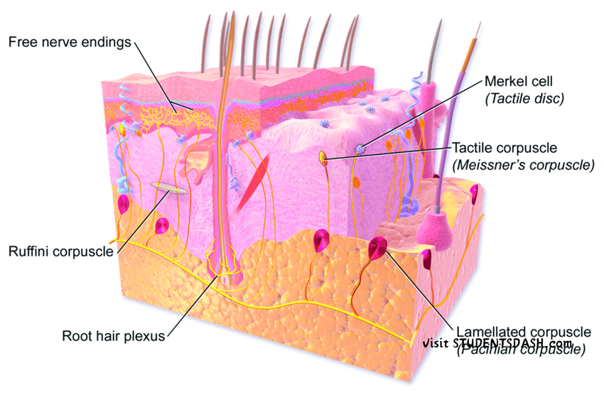
4. The Tactile Organ (Skin)
Functions of the Skin:
- Detects Touch and Pressure – Specialized nerve endings sense physical contact and pressure.
- Senses Temperature – The skin detects heat and cold, helping the body respond to temperature changes.
- Feels Pain – Pain receptors in the skin help detect injuries or harmful stimuli.
- Protects the Body – Acts as a barrier against bacteria, viruses, and harmful substances.
- Regulates Body Temperature – Sweating and blood vessel dilation help cool the body, while goosebumps help retain heat.
- Produces Vitamin D – When exposed to sunlight, the skin helps produce vitamin D for strong bones.
- Stores Fat and Water – The skin helps retain moisture and stores energy in fat cells.
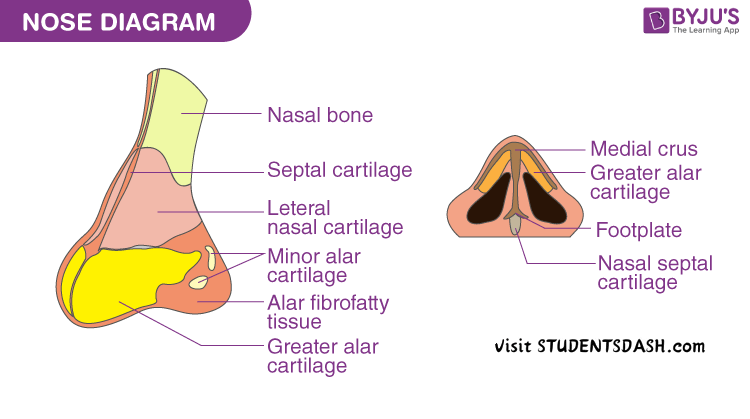
5. The Sense Organ of Smell (Nose)
Functions of the Nose:
- Detects Odors – Olfactory receptors in the nose identify different smells.
- Enhances Taste – Works with the tongue to help recognize flavors in food.
- Filters Air – The nose traps dust, germs, and pollutants using tiny hairs (cilia) and mucus.
- Moistens and Warms Air – Before air enters the lungs, the nose humidifies and warms it for better breathing.
- Aids in Breathing – The nose allows smooth airflow to the lungs for oxygen exchange.
- Triggers Reflexes – Sneezing helps remove irritants from the nasal passage.
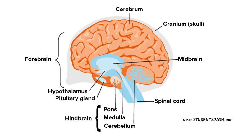
6. The Brain and Its Compartments
Functions of the Brain and Its Compartments:
- Cerebrum – Controls thinking, memory, reasoning, emotions, voluntary movements, and sensory processing.
- Cerebellum – Maintains balance, posture, and coordination of body movements.
- Brainstem – Regulates vital involuntary functions like breathing, heartbeat, and digestion.
- Hypothalamus – Controls body temperature, hunger, thirst, sleep, and emotions.
- Medulla Oblongata – Manages automatic functions like breathing, heart rate, and blood pressure.
- Thalamus – Acts as a relay center, sending sensory information to the appropriate brain areas.
- Pituitary Gland – Releases hormones that regulate growth, metabolism, and other body functions.
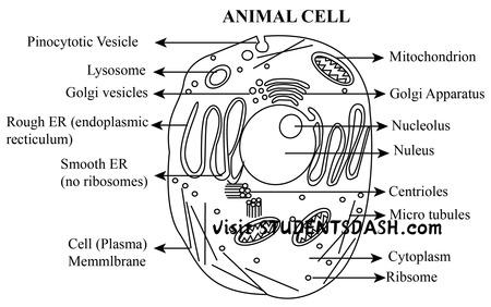
7. Animal Cell
Functions of the Animal Cell:
- Energy Production – The mitochondria generate energy (ATP) for the cell through cellular respiration.
- Protein Synthesis – The ribosomes produce proteins, which are essential for various cell functions.
- DNA Storage and Control – The nucleus contains genetic material (DNA) and controls cell activities.
- Transport of Materials – The endoplasmic reticulum (ER) helps transport proteins and lipids throughout the cell.
- Waste Removal – Lysosomes digest and remove waste products and old cell parts.
- Cell Division – The cell undergoes mitosis or meiosis for growth, repair, and reproduction.
- Cell Communication – The cell membrane facilitates communication with other cells and the environment.
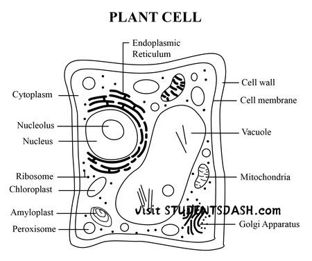
8. Plant Cell
Functions of the Plant Cell:
- Photosynthesis – Chloroplasts use sunlight to convert carbon dioxide and water into glucose (food) and oxygen.
- Energy Storage – The vacuole stores water, nutrients, and waste products, helping the plant maintain structure and function.
- Structural Support – The cell wall, made of cellulose, provides shape and rigidity to the cell, supporting the plant.
- Transport of Materials – Plasmodesmata allow the transport of water, nutrients, and information between plant cells.
- Growth and Development – The large central vacuole helps with cell expansion and growth by storing water and maintaining pressure.
- Protection – The cell wall acts as a protective barrier, shielding the plant cell from harmful microorganisms and environmental stress.
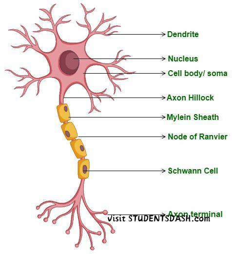
9. Neuron
Functions of the Neuron:
- Transmits Electrical Signals – Neurons carry electrical impulses (action potentials) throughout the nervous system to relay information.
- Processes Information – The brain and spinal cord receive and interpret signals from neurons to produce thoughts, memories, and actions.
- Coordinates Reflex Actions – Neurons control reflexes, allowing fast, automatic responses to stimuli, like pulling away from something hot.
- Connects Different Body Parts – Neurons form networks that link the brain, spinal cord, and various body parts, enabling communication and coordination.
- Releases Neurotransmitters – At synapses, neurons release neurotransmitters to communicate with other neurons or muscles.
- Supports Mental and Physical Functions – Neurons control activities like thinking, muscle movements, and regulation of body functions.
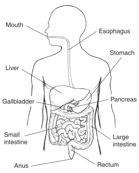
10. The Digestive System
Functions of the Digestive System:
- Breaks Down Food – The digestive system breaks down food into smaller, absorbable components (nutrients, sugars, fats, etc.) through mechanical and chemical processes.
- Absorbs Nutrients – After digestion, nutrients are absorbed into the bloodstream via the small intestine for use by the body.
- Eliminates Waste – The digestive system removes undigested food and waste products through the large intestine, ultimately excreting them as feces.
- Produces Digestive Enzymes – The pancreas and liver produce enzymes and bile to aid in the digestion and absorption of fats, proteins, and carbohydrates.
- Regulates Metabolism – The system ensures the proper digestion and absorption of food to maintain the body’s energy balance.
- Maintains Gut Health – The digestive system supports a healthy microbiome, which is essential for digestion, immune function, and overall health.
B. Differences between Plant and Animal Cells:
| Feature | Plant Cell | Animal Cell |
|---|---|---|
| Cell Wall | Present (made of cellulose) | Absent |
| Shape | Usually rectangular or square | Usually round or irregular |
| Chloroplast | Present (for photosynthesis) | Absent |
| Vacuole | Large central vacuole | Small or absent |
| Centrioles | Absent | Present |
| Lysosomes | Rarely present | Present |
C Functioning of the Neuron:
A neuron is a nerve cell responsible for transmitting electrical and chemical signals in the body. It functions in the following way:
- Reception of Stimulus: Dendrites receive signals from other neurons or sensory receptors.
- Transmission of Impulse: The electrical signal (action potential) travels through the axon.
- Synaptic Transmission: At the synapse, neurotransmitters are released to pass the signal to the next neuron or muscle.
- Response: The signal reaches the brain or muscles, leading to an action or reaction.
Neurons help in reflex actions, thinking, and coordination of body functions.